
Circuit Board Design – Custom Sensor
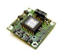
Using our electronics product development services, 3D Innovations was able to produce a schematic design to develop the circuit layout and determine Bill of Materials (BOM) requirements and cost. Gerber files were generated and used for the manufacturing process. While 3D Printing circuits was available, the conventional method for fabrication and assembly was used.
Integrating best practices for PCB design, development cost was reduced by 230% and prototypes built in several weeks saving 3-4 weeks in lead time. UL and FCC certifications were conducted to ensure testing compliance and approval. A production ready design was delivered for manufacturing.